© Copyright 2025. All Rights Reserved by Presto Stantest Pvt. Ltd.
18-May-2025
Presto Enviro
Electronic products fail for many reasons but temperature stress is one of the most common ones that people ignore during development. These circuit boards work fine in the lab but when they are used in actual harsh conditions, they may fail or create problems. Sudden temperature changes slowly affect the internal structure of the board. The damage usually starts small. Tiny cracks, weak solder joints, layer separation and eventually become a complete failure.
This is why thermal shock testing is discussed so often in electronics manufacturing. Companies want to know how their boards behave before products reach customers. Nobody wants field failures in automotive systems, telecom equipment, or industrial machines.
In this article, we will go through what thermal shock testing means for PCBs, why the test is important, how the testing procedure is carried out, and the standards generally followed during the process.
Thermal shock testing is used to check how a PCB behaves when exposed to rapid temperature changes. The board is shifted between extreme hot and cold conditions within a short time.
In real operating environments, electronics rarely stay at one stable temperature. A device may heat up during operation and cool down quickly once power is removed. Outdoor systems face even harsher conditions. Automotive electronics are a good example. Cold mornings, engine heat, long operating hours. The board keeps expanding and shrinking.
A PCB is made using multiple materials. Copper, epoxy resin, solder, fiberglass, and electronic components all react differently to heat. When the temperature changes too fast, those materials expand at different rates. That mismatch creates mechanical stress inside the board.
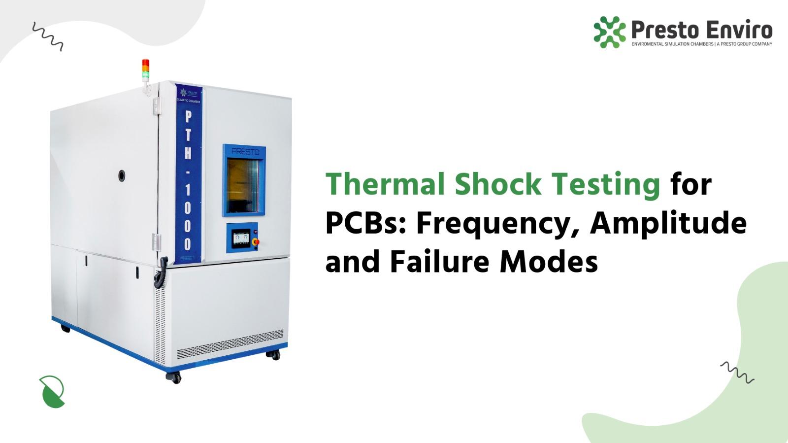
During thermal shock testing, the sample PCB is placed inside a thermal shock chamber. The chamber usually has separate hot and cold sections. The board moves repeatedly between both zones for a fixed number of cycles.
Some failures appear quickly during the test. Others take hundreds of cycles before becoming visible. Engineers normally inspect solder joints, vias, laminate bonding, and electrical continuity after testing.
Printed circuit boards are expected to operate in difficult environments now. Consumer electronics, industrial systems, telecom equipment, automotive modules. Almost every sector depends on compact electronic assemblies working reliably for long periods. The problem is that temperature stress slowly damages PCB structures from the inside.
For many companies, thermal shock testing is less about passing a requirement and more about avoiding expensive failures later.
The testing procedure follows a planned sequence. Exact settings may change from one industry to another, though the core process remains mostly similar.
The first step is sample preparation. Engineers inspect the PCB visually and sometimes perform electrical testing before the thermal cycles begin. Initial readings are recorded for comparison later.
After that, the chamber settings are configured. Thermal shock chambers generally have two or three temperature zones. One zone remains at high temperature while another stays at low temperature.
The temperature range depends on the application. Some tests may use -40°C to 125°C. High reliability products may require even tougher conditions.
Once setup is complete, the PCB starts moving between hot and cold zones repeatedly. The transfer happens quickly because the goal is to create sudden thermal stress instead of gradual heating.
A standard cycle usually includes:
This sequence is a continuous process and may run over 100 cycles which depends on the purpose of the product being manufactured or any specific requirements.
After testing, the PCB is inspected carefully by operators if there are any visible cracks, defects, solder fatigue and electrical failures. Some manufacturers also perform X-ray inspection to detect any internal damage that is challenging to see externally.
Thermal shock testing is usually performed according to industry standards. These standards help manufacturers follow consistent testing methods instead of using random conditions.
IPC Standard is a lesser-known standard used for thermal shock testing is IPC. IPC TM 650 includes different test methods related to PCB reliability and solder joint evaluation. PCB manufacturers refer to these guidelines during qualification and validation testing.
IEC 60068 is an international standard established by the International Electrotechnical Commission. It covers environmental testing procedures for electronic products including thermal shock and temperature cycling.
AEC Standards are also among the most commonly followed by automotive and electronics manufacturers. Vehicles and electronic devices face harsh environmental conditions which are hard to analyze sometimes when the product is in an early phase and that’s why these standards are important.
MIL Standards are mainly used by the military and aerospace industries for reliability testing. Equipment used in defense applications cannot afford unexpected failures during operation. Testing procedures are therefore more demanding.
JIDEC Standards are also widely followed for semiconductor and electronic component reliability testing. Many PCB assembly manufacturers refer to JEDEC methods during product qualification.
Different applications require different test conditions. A telecom PCB, for example, may not need the same thermal profile as an aircraft control board. That is why testing parameters are selected according to actual usage conditions.
Thermal shock testing allows the manufacturer to have a realistic idea of how a PCB will perform over time after being exposed to varying temperatures. The test brings to light characteristics that may not be identified on routine checks. It happens often when you try to add
A board that withstood thermal shocks is likely to be more reliable when put to use. This has a direct impact on the reliability of the product, maintenance price, and consumer confidence.
When companies are seeking reliable thermal shock testing systems, they typically prefer equipment manufacturers who have experience in making reliable equipment that will provide accurate and repeatable results. Presto Enviro is one of the leading thermal shock test chamber manufacturers in India, offering testing solutions for electronics, automotive, aerospace, and industrial applications. Businesses planning to improve PCB reliability testing can connect with our team for suitable chamber solutions based on their testing requirements.
Elevate your quality assurance process to new heights
Related Blogs

23-Sep-2026
Presto Enviro
Products are expected to work reliably for months or years, but manufacturers cannot always wait that long to find out how they will perform. Accelerated aging testing solves this problem by exposing products to controlled environmental conditions that speed up certain aging effects.
20-Sep-2026
Presto Enviro
Battery safety is not something manufacturers can check only after a battery is ready for use. Temperature, charging conditions and repeated use can change the way a battery behaves. In some cases, excessive heat can cause permanent damage or create serious safety risks.